
Pre-fabrication assurance

PCB design review before fabrication

An independent engineer checks your schematic, PCB layout and BOM before you commit to fabrication and assembly. Every finding is ranked by severity, explains its impact and cites the datasheet or standard behind it.

PRE-FABRICATION AUDIT SCOPE

What our PCB design review checks

Four places electronic design risk hides — in the schematic logic, on the pads, across the stack-up, and throughout the 3D layout.

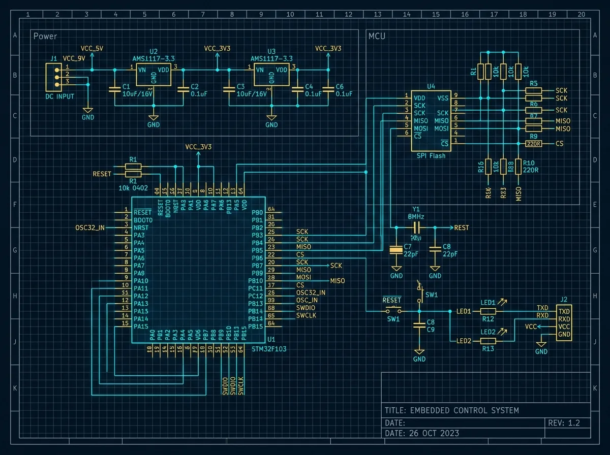
Schematic Logic & Power Rails
ELECTRICAL CHECK
TARGET:Logic Levels & Pinout

Schematic Logic & Power Rails

Pin connections, supply rail decoupling, pull-ups, and reverse protection verified before layout.

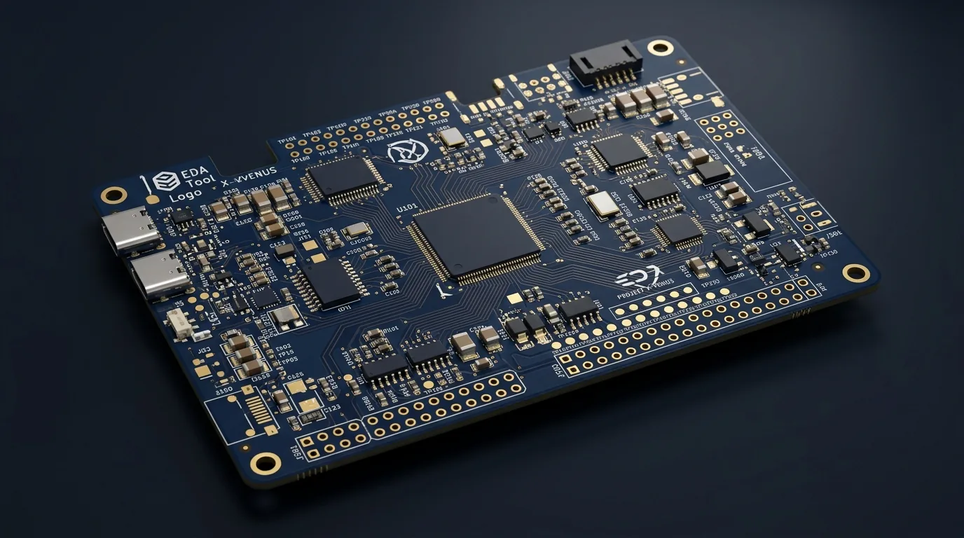
PCB 3D Layout & Clearances
PHYSICAL DRC
TARGET:Trace & Component Spacing

PCB 3D Layout & Clearances

Component height clearances, connector access, high-current copper width, and differential pairs.

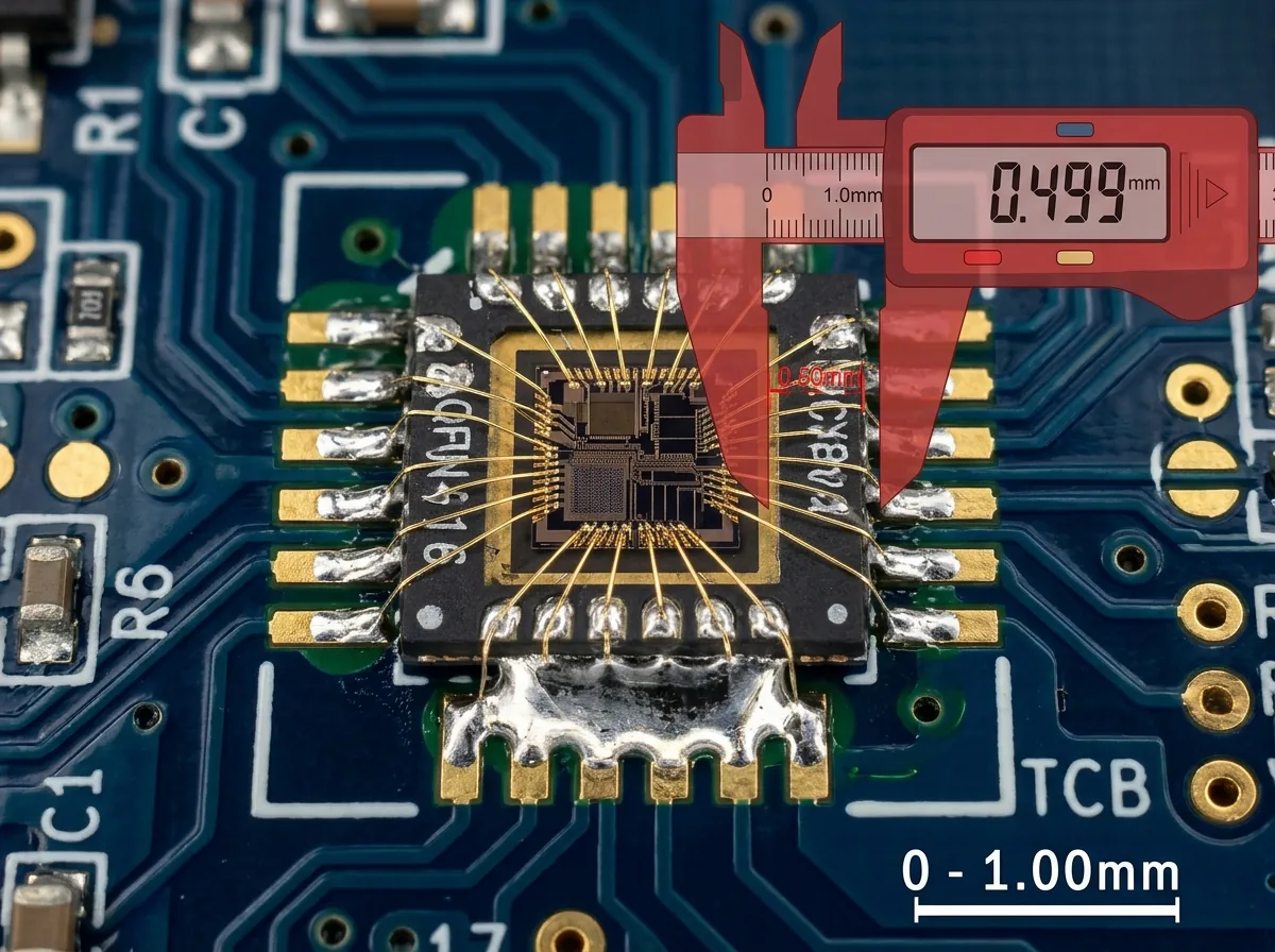
Footprint & Pad Geometry
SMT RELIABILITY
TARGET:Datasheet Pad Match

Footprint & Pad Geometry

Library land patterns audited against actual manufacturer physical package dimensions.

Multilayer Stack-Up & Vias
FABRICATION LIMITS
TARGET:Impedance & Core Vias

Multilayer Stack-Up & Vias

Layer count, copper weights, reference ground planes, and microvia aspect ratios.

Schematic review

Every net, rail and part checked against its datasheet.

  • Power entry, regulators, rails and decoupling
  • Pull-ups, strapping and boot pins, reset and enable timing
  • Absolute maximum ratings and recommended operating conditions
  • Reverse polarity, ESD and over-current on exposed connectors
  • Interfaces and connector pinouts

PCB layout review

What the schematic can't show.

  • Current paths: copper width, via counts and heat spreading
  • Return paths, reference planes and impedance-controlled routing
  • Clearance and creepage at higher voltages
  • Decoupling placement, connector access and keep-out areas
  • Footprints against manufacturer drawings and fab limits

BOM review

What gets bought matches what was designed.

  • Voltage, current and power ratings against the circuit
  • Capacitor dielectric and DC-bias derating
  • Footprint-to-package consistency
  • End-of-life, single-source and hard-to-buy parts
  • Schematic vs. BOM mismatches and missing DNF markings
THE REALITY OF ELECTRONICS AUDITING

Generic AI vs. PreBuild

Software AI models predict plausible-sounding words from text tokens. Electronic hardware obeys the laws of electromagnetics and physics. Here is why senior engineering review succeeds where automated AI copilots fail.

Generic AI & Chatbot Reviewers

Text-prediction without physical context

Trained on web text and generic forums. Prone to plausible hallucinations, misses critical silicon revisions, and cannot measure electromagnetic field behavior or assembly line tolerances.

PreBuild Human Engineering

Domain hardware engineers & empirical rules

Every design is analyzed by experienced hardware engineers with verified datasheet citations, real-world DFM fabrication rules, and rigorous net-by-net electrical validation.

Silicon Errata & Pin Muxing

Generic AI Pitfall

Hallucinates alternate pin configurations; assumes default GPIO mappings and completely misses manufacturer silicon errata notes.

PreBuild Engineering Check

Audits pin assignments against official silicon errata sheets, verifying hardware bootstrap states, pull-up/down ratios, and analog pin isolations.

DC Bias & Passive Derating

Generic AI Pitfall

Performs naive nominal value checks (e.g. "10µF capacitor is present"), unaware that small ceramic MLCCs lose up to 70% capacitance under DC bias voltage.

PreBuild Engineering Check

Validates actual effective capacitance under applied DC bias, ESR stability requirements for switch-mode regulators, and capacitor ripple current ratings.

Return Paths & Physical Parasitics

Generic AI Pitfall

Treats schematic connections as abstract mathematical nets; blind to split ground planes, excessive loop inductance, and return-current crosstalk.

PreBuild Engineering Check

Analyzes copper stack-up geometry, high-frequency return current paths, reference plane continuity, and critical decoupling loop inductances.

DFM & SMT Assembly Yield

Generic AI Pitfall

Repeats baseline EDA DRC numbers without context; misses tombstoning risks, thermal relief starving, solder wicking into vias, and tight connector access.

PreBuild Engineering Check

Audits footprint pad geometry against component datasheets, verifying solder mask dams, thermal balance, pick-and-place clearances, and fab limits.

A hardware prototype respin costs ₹50,000–₹3,00,000 and 4 to 8 weeks of lost lead time.
PREBUILD CATCHES WHAT TEXT MODELS MISS →

Who reviews your design

  • Senior hardware engineer leads every review
  • Power electronics, embedded systems and PCB design, from schematic to production
  • Every finding checked against its datasheet or standard

The report

A Design Assurance Report with a readiness status and every finding ranked by severity.

  • Critical
  • Significant
  • Verification
  • Improvement
FABRICATION RISK REDUCTION

Ready to find out before you fabricate?

Submit your design files securely under NDA. Receive your actionable Design Assurance Report before committing thousands to fab and assembly.